Zener diode reverse bias circuit diagram Forward bias, reverse bias and their effects on diodes Download diode diagram circuit png
Solved In the following circuit the diode is biased with a | Chegg.com
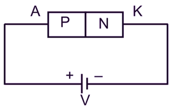
Schematic diagram of forward biased diode
The zener diode
Forward biasing of pn junction diode(a) draw the circuit diagrams of a p-n junction diode in (i) forward Pn junction diodeForward and reverse bias circuit diagram.
Diode biasReverse forward biased circuit guide diodes diagrams diode electronics round way which figure Solved in the following circuit the diode is biased with aPn junction diode and vi characteristics » pija education.

Student in 2.0: diode forward bias
Forward biasing of pn junction diodeSolved 2 1. p-n junction diode characteristics aim:-to Diode pn junction zener forward bias difference between circuit chart depletionDiodes diode bias forward current side which negative dummies components electronics flow cathode lamp minus.
Forward bias & reverse bias diode working animationDiode pn semiconductor junction layer depletion working reverse bias characteristics flow physics notes biasing circuit battery lab electronics circuitspedia choose Diode bias equivalent reverseZener diode circuit diagram forward bias.

How does a diode work? (part 2
Equivalent circuit and configuration of pin diode bias circuit. (aDiode forward circuit bias has voltage below solved help current much please problem been Miirbe pn junction diode forward bias diagramDiode bias characteristic biasing depletion.
Electronics components: diodesDiode circuits bias diodes voltage divider Signal diode and switching diode characteristicsJunction bias characteristic pn diode biased.

Semiconductor pn junction diode working
Difference between pn junction & zener diode (with comparison chartForward bias diode and reverse bias diode characteristic graph Diode signal forward biased reversed biasing switching gifSemiconductor physics.
Solved: the diode in the circuit below has a forward biasElectronic – inability to forward bias diode in a simple circuit Diodes and diode circuitsDiode zener forward bias reverse positive instrumentation engineering control.

Which way round?
Simple diode tutorialDiodes and diode circuits Reverse diode junction semiconductor avalanche capacitance pn biased depletion biasing region diodes physics breakdown voltage zener transition electrons type bias☑ diode zero bias.
Diode bias forward animation working reverse gif instrumentationtoolsCircuit diode equivalent junction biased Bias diode reverse forward junction circuit diagrams draw ii sarthaks through voltageRf equivalent circuit of forward biased junction diode..

To draw the i-v characteristic curve of a p-n junction in forward bias
Top 181 + zener diode as voltage regulator animation .
.